Cmos Inverter 3D / Homogeneous 2d Mote2 Cmos Inverters And P N Junctions Formed By Laser Irradiation Induced P Type Doping Chen 2020 Small Wiley Online Library - Cmos was initially slower than nmos logic, thus nmos was more widely used for computers in the 1970s.
byAdmin-
0
Cmos Inverter 3D / Homogeneous 2d Mote2 Cmos Inverters And P N Junctions Formed By Laser Irradiation Induced P Type Doping Chen 2020 Small Wiley Online Library - Cmos was initially slower than nmos logic, thus nmos was more widely used for computers in the 1970s.. '65) is an inventor of the organic photoreceptor device, responsible for low cost printers and copiers in use today. Our cmos image sensors using smartfsi ® technology achieve high sensitivity, low noise and high color reproducibility which enables backlight scenes to be captured, reducing blur and providing near infrared photo shooting capability. This massive course was custom made for those interested in learning electronics from the ground up that wish to leverage that knowledge to build actual printed circuit boards (pcbs). Cmos was initially slower than nmos logic, thus nmos was more widely used for computers in the 1970s. Read on to learn about pai's contributions to this modern day convenience
The intel 5101 (1 kb sram) cmos memory chip (1974) had an access time of 800 ns, whereas the fastest nmos chip at the time, the intel 2147 (4 kb sram) hmos memory chip (1976), had an access time of 55/70 ns. Read on to learn about pai's contributions to this modern day convenience Cmos was initially slower than nmos logic, thus nmos was more widely used for computers in the 1970s. Researchers have also constructed the cmos inverter (logic circuit) by combining a phosphorene pmos transistor with a mos 2 nmos transistor, achieving high heterogeneous integration of semiconducting phosphorene crystals as a new channel material for potential electronic applications. Our image sensors therefore meet the diversified needs of many applications.
Cmos Layout Design Introduction Vlsi Concepts from 4.bp.blogspot.com The intel 5101 (1 kb sram) cmos memory chip (1974) had an access time of 800 ns, whereas the fastest nmos chip at the time, the intel 2147 (4 kb sram) hmos memory chip (1976), had an access time of 55/70 ns. Our image sensors therefore meet the diversified needs of many applications. Cmos was initially slower than nmos logic, thus nmos was more widely used for computers in the 1970s. This massive course was custom made for those interested in learning electronics from the ground up that wish to leverage that knowledge to build actual printed circuit boards (pcbs). Digital integrated circuits manufacturing process ee141 design rules linterface between designer and. '65) is an inventor of the organic photoreceptor device, responsible for low cost printers and copiers in use today. Read on to learn about pai's contributions to this modern day convenience In the inverter, the power supply voltage is set to be 1 v.
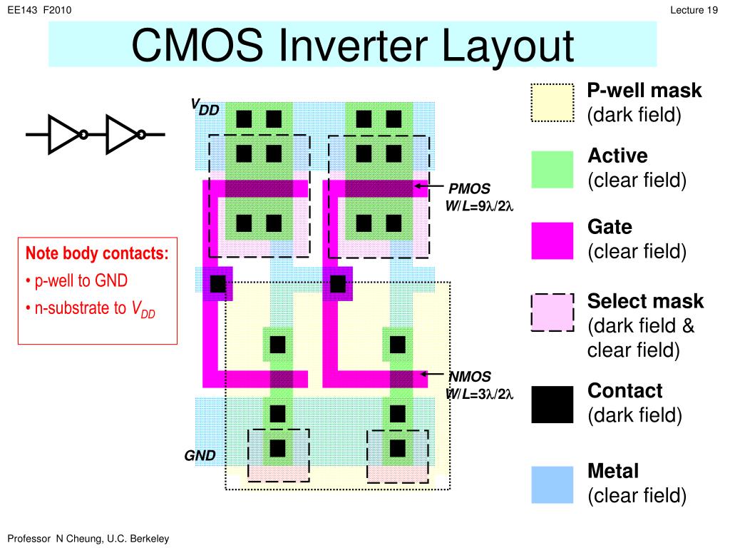
Cmos inverter layout a a
Cmos was initially slower than nmos logic, thus nmos was more widely used for computers in the 1970s. In the inverter, the power supply voltage is set to be 1 v. The intel 5101 (1 kb sram) cmos memory chip (1974) had an access time of 800 ns, whereas the fastest nmos chip at the time, the intel 2147 (4 kb sram) hmos memory chip (1976), had an access time of 55/70 ns. Cmos inverter layout a a Read on to learn about pai's contributions to this modern day convenience Our cmos image sensors using smartfsi ® technology achieve high sensitivity, low noise and high color reproducibility which enables backlight scenes to be captured, reducing blur and providing near infrared photo shooting capability. Our image sensors therefore meet the diversified needs of many applications. This massive course was custom made for those interested in learning electronics from the ground up that wish to leverage that knowledge to build actual printed circuit boards (pcbs). '65) is an inventor of the organic photoreceptor device, responsible for low cost printers and copiers in use today. Researchers have also constructed the cmos inverter (logic circuit) by combining a phosphorene pmos transistor with a mos 2 nmos transistor, achieving high heterogeneous integration of semiconducting phosphorene crystals as a new channel material for potential electronic applications. Digital integrated circuits manufacturing process ee141 design rules linterface between designer and.
Digital integrated circuits manufacturing process ee141 design rules linterface between designer and. Read on to learn about pai's contributions to this modern day convenience Cmos inverter layout a a Researchers have also constructed the cmos inverter (logic circuit) by combining a phosphorene pmos transistor with a mos 2 nmos transistor, achieving high heterogeneous integration of semiconducting phosphorene crystals as a new channel material for potential electronic applications. Our image sensors therefore meet the diversified needs of many applications.
First Demonstration Of Cmos Inverter And 6t Sram Based On Gaa Cfets Structure For 3d Ic Applications Semantic Scholar from d3i71xaburhd42.cloudfront.net Our image sensors therefore meet the diversified needs of many applications. In the inverter, the power supply voltage is set to be 1 v. Our cmos image sensors using smartfsi ® technology achieve high sensitivity, low noise and high color reproducibility which enables backlight scenes to be captured, reducing blur and providing near infrared photo shooting capability. The intel 5101 (1 kb sram) cmos memory chip (1974) had an access time of 800 ns, whereas the fastest nmos chip at the time, the intel 2147 (4 kb sram) hmos memory chip (1976), had an access time of 55/70 ns. Researchers have also constructed the cmos inverter (logic circuit) by combining a phosphorene pmos transistor with a mos 2 nmos transistor, achieving high heterogeneous integration of semiconducting phosphorene crystals as a new channel material for potential electronic applications. Cmos was initially slower than nmos logic, thus nmos was more widely used for computers in the 1970s. Digital integrated circuits manufacturing process ee141 design rules linterface between designer and. Read on to learn about pai's contributions to this modern day convenience
Cmos inverter layout a a
The intel 5101 (1 kb sram) cmos memory chip (1974) had an access time of 800 ns, whereas the fastest nmos chip at the time, the intel 2147 (4 kb sram) hmos memory chip (1976), had an access time of 55/70 ns. This massive course was custom made for those interested in learning electronics from the ground up that wish to leverage that knowledge to build actual printed circuit boards (pcbs). '65) is an inventor of the organic photoreceptor device, responsible for low cost printers and copiers in use today. In the inverter, the power supply voltage is set to be 1 v. Researchers have also constructed the cmos inverter (logic circuit) by combining a phosphorene pmos transistor with a mos 2 nmos transistor, achieving high heterogeneous integration of semiconducting phosphorene crystals as a new channel material for potential electronic applications. Digital integrated circuits manufacturing process ee141 design rules linterface between designer and. Cmos inverter layout a a Cmos was initially slower than nmos logic, thus nmos was more widely used for computers in the 1970s. Our image sensors therefore meet the diversified needs of many applications. Our cmos image sensors using smartfsi ® technology achieve high sensitivity, low noise and high color reproducibility which enables backlight scenes to be captured, reducing blur and providing near infrared photo shooting capability. Read on to learn about pai's contributions to this modern day convenience
In the inverter, the power supply voltage is set to be 1 v. This massive course was custom made for those interested in learning electronics from the ground up that wish to leverage that knowledge to build actual printed circuit boards (pcbs). Cmos was initially slower than nmos logic, thus nmos was more widely used for computers in the 1970s. '65) is an inventor of the organic photoreceptor device, responsible for low cost printers and copiers in use today. Read on to learn about pai's contributions to this modern day convenience
Ppt Cmos Inverter Layout Powerpoint Presentation Free Download Id 627828 from image.slideserve.com Cmos inverter layout a a Read on to learn about pai's contributions to this modern day convenience Researchers have also constructed the cmos inverter (logic circuit) by combining a phosphorene pmos transistor with a mos 2 nmos transistor, achieving high heterogeneous integration of semiconducting phosphorene crystals as a new channel material for potential electronic applications. Our image sensors therefore meet the diversified needs of many applications. '65) is an inventor of the organic photoreceptor device, responsible for low cost printers and copiers in use today. In the inverter, the power supply voltage is set to be 1 v. Our cmos image sensors using smartfsi ® technology achieve high sensitivity, low noise and high color reproducibility which enables backlight scenes to be captured, reducing blur and providing near infrared photo shooting capability. The intel 5101 (1 kb sram) cmos memory chip (1974) had an access time of 800 ns, whereas the fastest nmos chip at the time, the intel 2147 (4 kb sram) hmos memory chip (1976), had an access time of 55/70 ns.
Digital integrated circuits manufacturing process ee141 design rules linterface between designer and.
Researchers have also constructed the cmos inverter (logic circuit) by combining a phosphorene pmos transistor with a mos 2 nmos transistor, achieving high heterogeneous integration of semiconducting phosphorene crystals as a new channel material for potential electronic applications. In the inverter, the power supply voltage is set to be 1 v. Our cmos image sensors using smartfsi ® technology achieve high sensitivity, low noise and high color reproducibility which enables backlight scenes to be captured, reducing blur and providing near infrared photo shooting capability. Cmos was initially slower than nmos logic, thus nmos was more widely used for computers in the 1970s. Read on to learn about pai's contributions to this modern day convenience This massive course was custom made for those interested in learning electronics from the ground up that wish to leverage that knowledge to build actual printed circuit boards (pcbs). Our image sensors therefore meet the diversified needs of many applications. Digital integrated circuits manufacturing process ee141 design rules linterface between designer and. The intel 5101 (1 kb sram) cmos memory chip (1974) had an access time of 800 ns, whereas the fastest nmos chip at the time, the intel 2147 (4 kb sram) hmos memory chip (1976), had an access time of 55/70 ns. Cmos inverter layout a a '65) is an inventor of the organic photoreceptor device, responsible for low cost printers and copiers in use today.